USING THE TPU FUNCTION LIBRARY AND TPU EMULATION MODE
Order this document by TPUPN00/D
© MOTOROLA INC, 1997
MOTOROLA SEMICONDUCTOR PROGRAMMING NOTE
USING THE TPU FUNCTION LIBRARY AND TPU EMULATION MODE
By Jeff Wright and Mike Pauwels
1 Abstract
The Motorola time processor unit TPU is an on chip peripheral device used in the M68300 and
M68HC16 families of modular microcontrollers. This note describes the TPU function library and explains
how to use it. There is sufficient information for a user to select a new suite of functions from the
library, assemble them to run in TPU emulation mode, and submit the debugged assemblage as a new
TPU micro ROM code mask. Although background information is provided, the reader must refer to the
TPU Reference Manual TPURM/AD for details. This note is the first of a series. Subsequent notes
document functions in the library.
2 Introduction
The control store can contain up to 16 separate microengine programs (called TPU functions), each of
The procedures detailed in this note are intended for users who have found that the standard TPU functions
1. Assemble the new function set and have a custom TPU micro ROM mask made. A mask
4 TPU Control Store Organization
It is often neither possible nor necessary to fit 16 functions into the control store. When this is the case,
5 Emulation Mode Memory Map
The MC68334 microcontroller contains 1 Kbyte of internal RAM. With this device it is only possible to
In the MC68F333 microcontroller the 3.5 Kbyte TPURAM module is larger than the TPU microcode
Documentation for all TPU functions is available either in the TPU reference manual or in the form of
Due to limited microcode ROM size, compromises must often be made when selecting functions for inclusion
Critical operations determine the primary functions in the new set; the remaining task is to fit functions
7 Checking Code Size
Function A has a code size of 40 long words including subroutine file X
9 Assembling a New Function Set
TPUMASM.EXE is a microcode assembler that converts source code into hexadecimal code for the
Documentation for TPUMASM is available from Motorola technical representatives
1 After selecting the functions to include in a new set and obtaining the source code for these
Figure 5 Example TPU Library Source File
The example assembles six functions. The various fields of the example source file have the following
The %org assembler directive sets the microcode address for the start of the assembly. It is normal as
These two fields are actually microcode source code and labels that are commonly used in TPU functions.
This directive tells the assembler to include the TPU source code file of name funcname and assign
4. Invoke TPUMASM: To assemble the source file created above, type:
>TPUMASM filename
TPUMASM assembles filename and all include files and produces files named "filename.lst", "filename.S19",
APPENDIX C shows an example TPUMASM listing file. The listing file includes a memory map entry
10 Assembly Errors
Revision 3 and later revisions of TPUMASM have a multiple include capability; the assembler ignores
Assuming that all included files have been previously tested, and that there are no memory map violations,
11 Installing and Running Code in Emulation Mode
1 Configuring the on-chip Emulation RAM
The RAM base address must not conflict with other system memory or memory mapped peripherals.
RAMBAR can be written only once after reset. Enable the RAM module by writing the base address
2 Loading the code into RAM
When operating under a monitor such as CPU32Bug, microcode can be downloaded in S-record
3 Putting the TPU into Emulation Mode
While the TPU is in emulation mode, the RAM module is removed from the CPU memory map,
Once procedures for loading and configuring the TPU for emulation mode operation are completed, the
Can't make macro Usually occurs when a macro name is repeated. Use an editor to modify all
Entry Address in use Occurs when code overruns vectors. Too much code being used by microcode,
Entry Address already used Occurs when assembler attempts to write vector address in
WARNING DUPLICATE INCLUDE FILES NOT LOADED This is the only warning produced by
Each function entry takes the following form:
Mnemonic Name Code Size*
DCPM Degree Clock with Period Measurement 79
DIO Discrete Input Output 21
ITC Input Capture Transition Counter 36
OC Output Compare 39
PMA PMM Period Measurement Additional Missing 88
PPWA Period Pulse Width Accumulator 63
PSP Position Synchronized Pulse 96
PTA Programmable Time Accumulator 60
PWM Pulse Width Modulation 32
QDEC Quadrature Decode 29
QOM Queued Output Match 52
RWTPIN Read Write Timers and Pin 18
SM Stepper Motor Control 71
SPWM Synchronized PWM 54
*Code sizes of these functions include the subroutine file LINKCHAN (eight long words) If two or more of these
The time processor unit is a powerful, intelligent, on-chip peripheral. It is effectively a "co-microcontroller"
dedicated to performing complex timing and I/O tasks, and thus relieves the CPU of most of the overhead
associated with these tasks. Major TPU components are:
which can be executed on any one or more of the 16 TPU channels. The standard TPU control store
contains nine factory programmed functions that can perform a wide variety of control tasks. However
the standard functions may not be adequate for all applications. New TPU functions can be developed
either by Motorola or by the user to meet additional needs. In the future there may be new combinations
of functions released as standard TPU micro-ROM masks by Motorola.
do not ideally match the requirements of their application and who wish to investigate alternative
Motorola functions or who wish to integrate one or more functions they have written with standard functions.
The actual development of new TPU functions is beyond the scope of this document, but a microcode
training course from Motorola is available on request. It is strongly recommended that for
simplicity, new TPU users should attempt to fit the standard control store functions to their application
before taking this approach.
3 Running Alternate Function Sets
A user who wishes to use a new TPU function set has two options:
charge and minimum order quantity are associated with this option.
2. Make use of the special emulation mode built into the TPU. In emulation mode on-chip RAM
normally used by host CPU is loaded with TPU microcode and then configured for TPU use.
(see Figure 1)
In emulation mode the TPU can run a new function set from RAM with no loss
of performance.
and that loading emulation RAM with TPU code after power up takes time. In many cases emulation
mode provides the most suitable and cost effective approach to development and use
of new code.
The TPU control store consists of a contiguous 2 Kbyte block of micro ROM arranged as 512 long words
(See Figure 2).
This memory is divided into a microcode segment and an entry point segment. Each
TPU function has 16 word sized entry points associated with it; there are a total of 128 long words for
all 16 possible functions. Entry points are arranged in order by function number 0 to 15. Function numbers
are assigned to functions as part of the assembly process. Each entry point acts as a vector, forcing
function execution to begin at a known address. The entry point vector used at the start of each
channel service depends on several conditions. Refer to the TPU Reference Manual TPURM/AD for
more information.
the memory area occupied by entry points of unused function numbers is available for extra microcode
space. Begin function number assignment with 15 and work down so that any unused entry point segment
is contiguous with the normal microcode segment. This is the most efficient use of the available
space. Figure 3
shows unused entry points being used for additional opcode space.
When the TPU enters emulation mode, internal microcontroller RAM is dedicated to the TPU and replaces
the control store ROM. Most microcontrollers currently available with a TPU have a full 2 Kbytes
of internal RAM which allows complete emulation of the control store. Figure 2 shows the equivalent
host CPU byte addresses that are used to load internal RAM with TPU microcode before invoking emulation
mode.
emulate half the TPU control store at any one time.
Figure 4shows emulation memory map and equivalent
RAM addresses for this device.
control store. In this device, only a portion of the RAM is used for TPU emulation, but the entire RAM
is removed from the CPU memory map during emulation. In the future there may be other microcontrollers
with on-chip RAM modules that are larger than the TPU microcode control store, however the
emulation mode memory map will never be larger than the control store map.
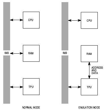
Figure 1 On Chip RAM Configuration
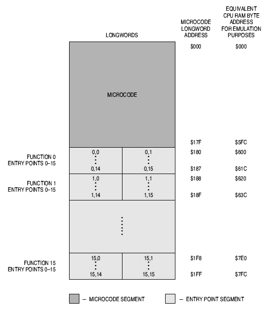
Figure 2 TPU Control Store and 2 Kbyte Emulation RAM Map
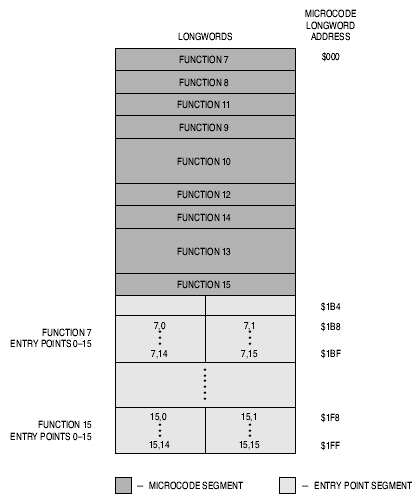
Figure 3 Extending Microcode Segment By Means of Unused Entry Points
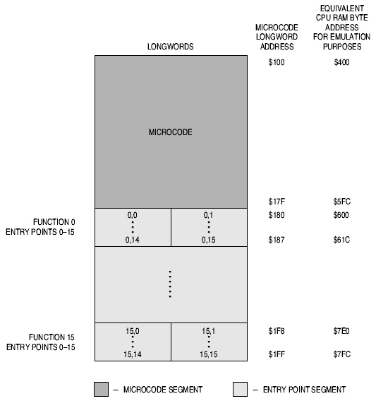
Figure 4 1 Kbyte Emulation RAM Memory Map
6 Selecting Functions from the TPU Library
To support changing TPU application requirements and to allow inclusion of customer-defined TPU
functions, Motorola has established a TPU function library. The function library is a collection of TPU
functions written for easy assembly in combination with each other or with custom functions. The library
currently includes all functions from the standard microcode ROM and several others that offer additional
functionality (See Appendix B). Other functions are being developed the list of functions will continue
to grow as Motorola responds to requests for new features.
a separate application report. Source code for functions, which is required to combine them into a new
set, is available from the Motorola bulletin board or via your local Motorola technical representative.
in a new set. There are typically one or more critical operations for a given application that must
have the best possible performance and several other operations with lower performance demands.
suitable for other operations into available code space. If there is not enough space for all the functions
initially desired, a performance/code size trade-off must be made. For example, there may be two functions
that perform essentially the same operation, but one is more sophisticated and therefore more attractive
to the user. Sophisticated functions typically require more code space than simpler functions.
By selecting the simpler function, and perhaps accepting a small increase in CPU overhead, the required
functionality can be made to fit in the available space. It might also be possible to fulfill two sets
of requirements with a single function, perhaps with a performance limitation that can be tolerated in the
given application. For example the Queued Output Match function can be used to generate a PWM
signal or to control an output pin, and thus might replace the PWM and DIO functions.
All the TPU functions in Appendix B have a code size given in long words that includes the entry points.
As will be explained later two additional long words are always required when combining these functions.
The code space occupied is equal to the sum of the code sizes of the selected functions plus two --
this total must be less than or equal to the 512 long word limit 256 for a device with 1 Kbyte of RAM.
When more than one of the selected functions include call the same subroutine file the code sizes of
all the functions except one can be reduced by the size of the subroutine file The following example
shows both cases:
Function B has a code size of 35 long words
Function C has a code size of 50 long words including subroutine file Y
Function D has a code size of 63 long words including subroutine file X
Subroutine X consists of 10 long words
Subroutine Y consists of 6 long words
Total code size after combining functions A B C and D is
40 35 50 63 10 2 180 long words
8 Obtaining Source Code from the Bulletin Board
The source code for all library functions is available on Motorola bulletin boards The bulletin board
number in the United States is 512 891 3733 The European bulletin board is available through the
Motorola Munich sales office consult your representative for the number Log on to the bulletin board
as usual follow the directions to the TPU section and then download source files and documentation.
Once desired functions have been selected and total code size has been verified to be within the 512
long word limit source code for individual functions must be assembled to generate executable code
Follow the procedures below using the freeware TPU assembler TPUMASM.
TPU microengine It runs on IBM PC and compatible computers and produces a listing file an S 19 file
a symbol table and a debugging file The symbol table and the debugging file are used only by the TPU
debugger.
The following procedures provide sufficient information for the successful compilation of a new function
set from existing previously tested functions.
functions the user must write the source file that will be assembled by TPUMASM
2 As part of the assembly process function numbers must be assigned to the selected functions
Each function in the set must have a unique number from 15 to 0 Assign function numbers from
15 down to make most efficient use of microcode space When including functions from the
standard set it is not necessary to keep the same function number documented in the TPU reference
manual Function numbers assigned here are those that the CPU must write into the
channel function select registers when the TPU is to execute a function on a specific channel
Selection of the function number for a given function is not related to the channel number selected
to execute the function.
3 After the filename and function numbers have been selected a source file can be created The
file should take the form shown in Figure 5
%org 0.
End_of_phase: end.(* provide common exit points for *)
End_of_link: (* library functions *)
chan neg_lisl;
end.
%Include �qdec.uc'; function = 15.
(* include function qdec as function number 15 *)
%Include �pwm.uc'; function = 14.
(* include function pwm as function number 14 *)
%Include �ppwa.uc'; function = 13.
(* include function ppwa as function number 13 *)
%Include �qom.uc'; function = 12.
(* include function qom as function number 12 *)
%Include �dio.uc'; function = 11.
(* include function dio as function number 11 *)
%Include �oc.uc';function = 10.
(* include function qdec as function number 10 *)
(* This is the end of the file *)
meanings:
(* this is a comment *)
%org 0
in this example to set the origin to zero when assembling a new function set for emulation in a 2 Kbyte
RAM module. For the MC68334 device which has a 1 Kbyte RAM module, set the microcode origin to
100.
End_of_phase: end.
End_of_link: chan neg_lsl;
end.
They have been separated from the individual functions and are called using the common label
names. This allows all the functions to share the same two instructions thus saving code space. These
instructions must always be included when assembling library functions; they fill the extra two long
words that are added when calculating whether functions fit into the 512 long word code space
%include �funcname';function = funcnumber.
it the function number funcnumber. The function number is that chosen in step 2; it can be entered in
hexadecimal or decimal form. Function position in the combined code is determined by the order of the
include directives and not by function number; this is shown in Figure 3 where the functions appear
to be out of order.
"filename.SYM" and "filename.TAB". If errors are generated, they are displayed during assembly
and are also present in the listing file.
list and identifier cross reference. All microcode fields include a "+" in the first column and are written
as eight character (32 bit) hexadecimal numbers
To maximize code efficiency, several functions may share a common subroutine. To avoid code duplication
when assembling functions together, such a subroutine is often in a separate file which is incorporated
via an include directive in the individual function source files. An example of this approach is
the Link chan subroutine which is called by several of the library functions. This subroutine is in a file
of its own called Linkchan and the appropriate directive %include Linkchan is present in all the functions
that call it.
second and subsequent inclusions of the same file but appends a warning message at the end of assembly
to protect against an attempt to include two different files of the same name. Earlier versions of
the assembler do not have this capability; when functions that call the same subroutine are assembled
together illegal label errors occur, and it is necessary to remove the include directive from all but
one of the source files.
there should be no assembly errors. However, in case an error does occur, the most common
assembly error messages together with corrective action for each type of error are listed in Appendix A
Installing and running code in emulation mode involves three steps:
Reset clears the RAM base address register RAMBAR. Since RAMBAR contains both the array
base address and the RAM module enable bit, a new base address must be set up and the
RAM module must be enabled before the RAM can be loaded.
The RAM module (1K or 2K) can reside on any 2 Kbyte boundary in the MCU address
map. In the case of the 1-Kbyte module, the RAM resides in the upper 1 Kbyte of the 2 Kbyte
address block.
and enable bit with a single word write operation. Make certain that all stack pointers
point to addresses elsewhere is system memory before attempting to execute a load procedure.
Refer to the documentation for the RAM module.
There are two methods of writing assembled microcode into emulation RAM:
form from the host. The specific host communication program used to communicate with
the monitor must provide a download facility for this purpose.
When operating under user program control, microcode must be assembled or compiled in the
form of a data table by the host CPU program, then moved into emulation RAM under CPU program
control. Time taken to move microcode into RAM is the only penalty for using emulation
mode rather than a custom microcode mask, and the penalty should only be incurred once after
reset.
After RAM has been configured and loaded with microcode, it is necessary to enable RAM emulation
mode for TPU access. To enable emulation mode, use either the monitor or a control
program to set the EMU bit in the TPU module configuration register. Since the module configuration
register contains write-once fields, it is also necessary to write the TPU prescaler control
fields at the same time. Should a subsequent reset occur the configuration register must be
rewritten, but it may not be necessary to reload emulation RAM. See the TPU Reference Manual
TPURM/AD for more information about the module configuration register.
and the vacated address space may be allocated to other devices.
TPU will run the suite of newly installed functions as though they were contained in the control store
ROM. To run the functions, the CPU must set up control registers and parameter RAM as explained in
the documentation for each function.
Appendix A TPUMASM Error Messages
Following is a list of TPUMASM error messages, probable causes of error. and corrective action.
Can't open file File not found by TPUMASM. Check current directory.
Illegal label Usually occurs when a label name is repeated. If two source files are using the
same label, use an editor to modify all instances of the label in one of the files. If the same file is included
more than once, illegal label errors may occur. See main text.
instances of the label in one of the files.
or function number too small. Recheck code size and number all functions from 15 down.
space used by microcode. Recheck code size and number all functions from 15 down.
the assembler. It occurs when there has been an attempt to include the same file two or more times.
The second and subsequent includes will have been ignored.
Appendix B TPU Function Library
Following is a description of the TPU function library at the time this note was prepared. New functions
are continually being developed. The reader is encouraged to obtain the most recent list from the Motorola
bulletin board. Existing functions may also be revised from time to time. A series of programming
notes is being written to document each of the functions.
A summary of the major features of the function. Function capabilities are not fully described in these notes.
This input function reads a signal from a toothed wheel sensor, and inserts a selected number of counts at even intervals
between signals. The resulting count driven on TCR2 continues to a fixed maximum, and then resets providing
an approximation of the angle of wheel shaft rotation. The period of the last two teeth is maintained in a 23 bit parameter.
Stall indication is provided via a host interrupt.
Allows a TPU channel to be used as a digital I/O pin. When the pin is configured as an input, a transition detector can
indicate a change of state to the CPU. Additionally, the host can define a sample rate at which the pin is to be tested
and pin state reported to the CPU. The pin state parameter contains the last 16 samples, allowing debounce or noise
rejection to be accomplished.
This function can perform a basic input capture operation, where a timer value is captured on a pin transition and reported
to the CPU. In addition, a user can specify a number of transitions to be counted. On each transition, the captured
time is returned to the CPU. When the required number of transitions has been counted, the last transition time
is stored in a different location, and a CPU interrupt request is made. At this point, the function can also automatically
link to a number of other TPU channels. The sequence of counting transitions can be programmed to occur once only
or continuously.
This output function generates a rising edge, a falling edge, or a toggle on the channel pin in one of two modes:
I. When a single edge occurs a programmable period after a user defined time. A start condition can also be specified
allowing pulse generation.
II. On receiving a link from another channel, OC generates a continuous 50% duty cycle
waveform with a period that is calculated, without CPU intervention, by multiplying a period obtained from another TPU
channel by a user-specified ratio parameter. The OC function can also provide the CPU with current TCR values.
This input function, primarily designed for engine control, measures the period in TCR1 clocks between regularly occurring
input transitions, and makes this period available for use by other functions or by the CPU. PMA mode detects
when the period between transitions is less than a user-specified fraction of the last normal period additional transitions.
PMM mode detects when the period between transitions is greater than a user-specified fractional multiple of
the last normal period missing transitions. After a programmable number of additional or missing transitions are detected,
the function resets the TCR2 timer counter and interrupts the CPU. The PMA PMM process is continuous and
requires no CPU intervention once configured.
This input function accumulates a 24 bit sum of either the period or the high time pulse width of an input signal over a
programmable number of periods/pulses 1 to 255. An interrupt request is made when the specified number of periods/
pulses has elapsed. The period/pulse width is sampled at a rate defined by the user, and the incomplete sum is available
to the user. By linking to an OC channel an output signal can be generated that is proportional to that applied to the
PPWA channel.
This output function generates pulses of variable length at specified angles when an angle clock has been fed into the
TCR2 input pin. Angle clock period is measured in TCR1 clocks using the PMA/PMM function on another channel.
The function uses a fractional multiply on the PMA/PMM period to accurately position pulses to a higher angular resolution
than that provided by the TCR2 angle clock. The rising edge of the pulse is always defined as an angle and the
falling edge can be specified as a second angle or as a time after the rising edge. Once configured, the PSP function
continuously generates pulses based on the latest period information obtained from a PMA/PMM channel without CPU
intervention.
This input function accumulates a 32 bit sum corresponding to the period the high time or the low time of an input
signal over a programmable number (1 to 255) of periods pulses. A CPU interrupt request is made and optionally
links when the specified number of periods/pulses elapses. This function is an extension of the PPWA function but it
has no programmable update rate.
This function generates a pulse width modulated waveform. The period and/or high time of the waveform can be
changed at any time by the CPU. The function supports both 0 and 100% duty cycles. Very high resolution can be
obtained depending on the frequency required.
This input function uses two channels to decode a pair of out-of-phase signals in order to present the CPU with directional
information and a position value. It is particularly suitable for use with slotted encoders employed in motor control.
The function derives full resolution from the encoder signals and provides a 16-bit position counter with rollover/under
indication via an interrupt.
This output function lets the user set up multiple output events in a variable-sized match table which is processed by
the TPU without CPU intervention. The pin response for each output event is independently programmable. This allows
multiple entries with the same pin response to be used, which effectively increases the range of a single output event.
The function includes loop modes, which cycle through the table continuously, or a programmable number of times. A
link can be used to trigger the function.
This function allows a TPU channel to be used as a digital I/O pin. It also allows the CPU to read both TCRs and to
selectively write to each TCR. Upon receipt of a link, the function reads the timers, updates the channel pin, and interrupts
the CPU. The function can also be used to manipulate the timers only with no effect on the pin, thus making it
suitable for use on a channel that has its pin controlled by another channel.
This function allows a sequential group of up to eight TPU channels to be used to drive a stepper motor. Once the function
is configured, the CPU need only specify the required position and the function automatically accelerates and decelerates
the motor to the desired position. The algorithm provides 14 programmable step rates for linear acceleration
and deceleration control.
This output function generates a PWM waveform. The CPU can change the period and or the high time of the waveform
at any time. SPWM differs from the PWM function in that rising edges have a programmable time relationship to transitions
on another TPU channel, including other SPWM channels. Three different operating modes allow the function
to maintain complex timing relationships between channels without CPU intervention. 0 and 100% duty cycles are
not supported.
functions are used, the code sizes of all but one can be reduced by eight long words.
Appendix C EXAMPLE TPUMASM LISTING
$ 1 (* ****************************************************************** *)
$ 2 (* TEST.ASC - standard exits plus one include *)
$ 3 (* ****************************************************************** *)
$ 4 %org 0.
$ 5
+000/3FFFFFFE 6 End_of_phase: end.
$ 7
$ 8 End_of_link: chan neg_lsl;
+001/7FFFFEFE9 end.
$ 10
$ 11 %include �sqw.uc'; function = $F.
$ 1 1 (* Translated by TPUCNV.EXE V0.4 *)
$ 1 2 (*******************************************************************)
$ 1 3 (* *)
$ 1 4 (* Function: SQW - SQUARE WAVE *)
$ 1 5 (* *)
$ 1 6 (* Creation Date: 03/Mar/92 From: NEW *)
$ 1 7 (* *)
$ 1 8 (* Author: Amy Dyson *)
$ 1 9 (* *)
$ 1 10 (* Description: *)
$ 1 11 (* ------------ *)
$ 1 12 (*SQW produces a continuous square wave after initialization.The *)
$ 1 13 (*user chooses the period by writing the parameter HIGH_TIME in ram. *)
$ 1 14 (* (High time and low time are the same.) HIGH_TIME must be between *)
$ 1 15 (* $0000-$8000. *)
$ 1 16 (* *)
$ 1 17 (* Updates: By: Modification: *)
$ 1 18 (* -------- --- ------------- *)
$ 1 19 (* 11/Apr/93 JL Converted to new syntax. *)
$ 1 20 (* *)
$ 1 21 (*---------------------------------------------------------------- *)
$ 1 22 (* Standard Exits Used:- End_Of_Phase: N End_Of_Link: Y *)
$ 1 23 (* *)
$ 1 24 (* External Files included: NONE *)
$ 1 25 (* *)
$ 1 26 (* CODE SIZE excluding standard exits = 11 LONG WORDS *)
$ 1 27 (*---------------------------------------------------------------- *)
$ 1 28 (* *)
$ 1 29 (* *)
$ 1 30 (********** This Revision: REV B ********)
$ 1 31 (* *)
$ 1 32 (******** LAST MODIFIED: 11/Apr/93 BY: Jeff Loeliger *******)
$ 1 33 (* *)
$ 1 34 (***************************************************************** *)
$ 1 35
$ 1 36
$ 1 37 (*()()()()()()()()()() DATA STRUCTURE ()()())()()()()()()()()()() *)
$ 1 38 (* *)
$ 1 39 (* name: Written By: Location Bits: *)
$ 1 40 (* ----- ----------- --------------- *)
$ 1 41 (* HIGH_TIME_SQW CPU Parameter0 0.15 *)
$ 1 42 (* High time of period. (Also the low time, since *)
$ 1 43 (* this is a square wave.) HIGH_TIME_SQW cannot *)
$ 1 44 (* be greater than $8000. *)
$ 1 45 (* *)
$ 1 46 (* hsr1 hsr0 Action *)
$ 1 47 (* ---- ---- ------ *)
$ 1 48 (* 1 1 Initialize continuous square wave *)
$ 1 49 (* *)
$ 1 50 (* *)
$ 1 51 (* Links Accepted: NO Links Generated: NO *)
$ 1 52 (* *)
$ 1 53 (* Interrupts Generated After: No interrupts generated *)
$ 1 54 (* *)
$ 1 55 (*()()()()()()()()()()()()()()()()()()()()()()()()()()()()()()()() *)
$ 1 56
$ 1 57
$ 1 58 (*++++++++++++++=++++ PARAMETER MACROS +++++++++++++++++++++++++ *)
$ 1 59
$ 1 60 %macro HIGH_TIME_SQW �prm0'.
$ 1 61 (*++++++++++++++++++++++++++++++++++++++++++++++++++++++++++++++++ *)
$ 1 62
$ 1 63
$ 1 64 (*================================================================ *)
$ 1 65 (*||||||||||||||||||| MICROCODE STARTS BELOW ||||||||||||||||||| *)
$ 1 66 (*VVVVVVVVVVVVVVVVVVV--------------------------VVVVVVVVVVVVVVVVVVV *)
$ 1 67
$ 1 68
$ 1 69 (***************************************************************** *)
$ 1 70 (* *)
$ 1 71 (* ENTRY name: INIT_SQW *)
$ 1 72 (* *)
$ 1 73 (* STATE(S) ENTERED: S1 *)
$ 1 74 (* *)
$ 1 75 (* PRELOAD PARAMETER: HIGH_TIME_SWQ *)
$ 1 76 (* *)
$ 1 77 (* ENTER WHEN: HSR = %11 *)
$ 1 78 (* *)
$ 1 79 (* ACTION: set time base as TCR1, set pin high, and pac to toggle *)
$ 1 80 (* pin after each match. Write the current time + the *)
$ 1 81 (* HIGH_TIME to the mer. Negate latches. Enable service *)
$ 1 82 (* requests. *)
$ 1 83 (* *)
$ 1 84 (***************************************************************** *)
$ 1 85 %entry name = INIT_SQW; start_address *; disable_match;
$ 1 86 cond hsr1=1,hsr0=1,lsr=x,m/tsr=x,pin=x,flag0=x;
$ 1 87 ram p <-@HIGH_TIME_SQW.
$ 1 88
$ 1 89 chan TBS:= out_m1_c1, (* pin is output, use TCR1 *)
$ 1 90 PAC:= toggle, (* toggle pin on match *)
$ 1 91 pin:= high, (* initialize pin as high *)
+002/BFFF477C 1 92 enable_mtsr. (* enable m/tsr requests *)
$ 1 93
$ 1 94 au ert:= tcr1+p; (* write current time + *)
$ 1 95 chan write_mer, (* high time to mer *)
$ 1 96 neg_mrl, neg_tdl, neg_lsl; (* negate latches *)
+003/58583EFE 1 97 end. (* end of S1 *)
$ 1 98
$ 1 99 (*************************************************************** *)
$ 1 100 (* *)
$ 1 101 (* ENTRY name: MATCHED_SQW *)
$ 1 102 (* *)
$ 1 103 (* STATE(S) ENTERED: S2 *)
$ 1 104 (* *)
$ 1 105 (* PRELOAD PARAMETER: HIGH_TIME_SWQ *)
$ 1 106 (* *)
$ 1 107 (* ENTER WHEN: HSR = %00 m/tsr=1 lsr=X flag0=X pin=X *)
$ 1 108 (* *)
$ 1 109 (* ACTION: Write HIGH_TIME_SQW + last match time to mer, neg_mrl. *)
$ 1 110 (* *)
$ 1 111 (******************************************************************)
$ 1 112 %entry name = MATCHED_SQW; start_address *; disable_match;
$ 1 113 cond hsr1=0,hsr0=0,lsr=x,m/tsr=1,pin=x,flag0=x;
$ 1 114 ram p <-@HIGH_TIME_SQW.
$ 1 115
$ 1 116 au ert:= ert + p; (* write last match time + *)
$ 1 117 chan write_mer, (* high time to mer *)
$ 1 118 neg_mrl, neg_tdl, neg_lsl; (* negate latches *)
+004/5C583EFE 1 119 end. (* end of S2 *)
$ 1 120
$ 1 121 (******************************************************************)
$ 1 122 (* UNUSED STATES *)
$ 1 123 (******************************************************************)
$ 1 124
$ 1 125 %entry name = UNUSED_SQW; start_address END_OF_LINK; disable_match;
$ 1 126 cond hsr1=0,hsr0=1,lsr=x,m/tsr=x,pin=x,flag0=x.
$ 1 127
$ 1 128 %entry name = UNUSED_SQW; start_address END_OF_LINK; disable_match;
$ 1 129 cond hsr1=1,hsr0=0,lsr=x,m/tsr=x,pin=x,flag0=x.
$ 1 130
$ 1 131 %entry name = UNUSED_SQW; start_address END_OF_LINK; disable_match;
$ 1 132 cond hsr1=0,hsr0=0,lsr=1,m/tsr=0,pin=x,flag0=x.
$ 12
$ 13
$ENTRY TABLE
$===========
+1F8/E801E801 UNUSED_SQW UNUSED_SQW
+1F9/E8010002 UNUSED_SQW INIT_SQW
+1FA/00040004 MATCHED_SQW MATCHED_SQW
+1FB/00040004 MATCHED_SQW MATCHED_SQW
+1FC/E801E801 UNUSED_SQW UNUSED_SQW
+1FD/E801E801 UNUSED_SQW UNUSED_SQW
+1FE/00040004 MATCHED_SQW MATCHED_SQW
+1FF/00040004 MATCHED_SQW MATCHED_SQW
$
$ROM MAP
$=======
$ 0123456789ABCDEF
$ ----------------
$00 XXXXX...........
$01................
$02................
$03................
$04................
$05................
$06................
$07................
$08................
$09................
$0A................
$0B................
$0C................
$0D................
$0E................
$0F................
$10................
$11................
$12................
$13................
$14................
$15................
$16................
$17................
$18................
$19................
$1A................
$1B................
$1C................
$1D................
$1E................
$1F........EEEEEEEE
$20................


$====> 5 U_instructions generated
$====> 8 Entry lines generated
$====> 13 Total
$
$ENTRY TABLE MAP
$===============
$180 .. .. .. .. .. .. .. ..
$188 .. .. .. .. .. .. .. ..
$190 .. .. .. .. .. .. .. ..
$198 .. .. .. .. .. .. .. ..
$1A0 .. .. .. .. .. .. .. ..
$1A8 .. .. .. .. .. .. .. ..
$1B0 .. .. .. .. .. .. .. ..
$1B8 .. .. .. .. .. .. .. ..
$1C0 .. .. .. .. .. .. .. ..
$1C8 .. .. .. .. .. .. .. ..
$1D0 .. .. .. .. .. .. .. ..
$1D8 .. .. .. .. .. .. .. ..
$1E0 .. .. .. .. .. .. .. ..
$1E8 .. .. .. .. .. .. .. ..
$1F0 .. .. .. .. .. .. .. ..
$1F8 EE EE EE EE EE EE EE EE
$
$===> 16 Entries generated
$
$LABELS:
$=======
$Label Hex dec
$===== === =====
$END_OF_LINK 001 0/ 1
$END_OF_PHASE 000 0/ 0
$
$MACROS:
$=======
$macro body
$===== =======
$HIGH_TIME_SQW PRM0
$
$ NO ERRORS
$ ---------